ASIC/FPGA Design and Verification Out Source Services
VHDL IP Stack
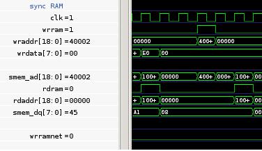
Replacing the asynchronous SRAM with a synchronous write memory.
- The asynchronous RAM was probably the only choice available on the evaluation board, when the design was first done.
- Today synchronous memories are common and good practice.
- I selected a memory with synchronous write and asynchronous read. This model is very popular with FPGA memories.
- Usually the read data output is sampled. This is what I did. The data is sampled when the read RAM strobe is asserted.
- The code is now more synthesis friendly as former asynchronous memory implementation used some logic on the clock to generate a write pulse.
-
To go back to the VHDL IP main page: main .
Contact me now at: |