ASIC/FPGA Design and Verification Out Source Services
SD slave with Samsung flash (k9f1208)
read burst: the command phase.
-
This page is part of SD project:
go -->
-
This project was translated to VHDL from a free SD verilog project,
which is also available in this site:
go -->
The test-bench and RTL code were translated
to VHDL. A read burst was also added to
improve the speed of a read access from flash.
A general description of a read burst flow can
seen in the following link:
go -->
This page describes the command phase of the read
burst.
-
First commands 23 and 18
(marker A and B) are
driven on the SD lines, by the test-bench:
-
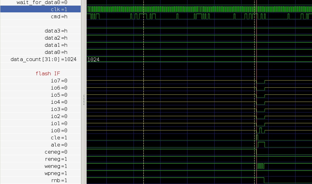
Once the SD commands are parsed, by the DUT's SD
logic, the flash state machine starts it work
(red marker). It
places the flash read command followed by address (
not shown in this wave).
-
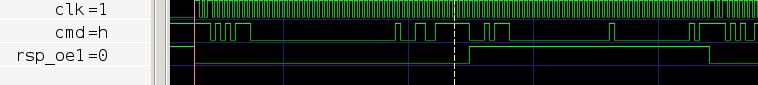
The next wave shows the SD lines activity, first
signals, which are driven
by the bench, with SD command 23. It is then
followed by the DUT's response.
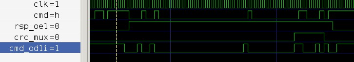
Due to synthesis consideration, the three state
statement, in the VHDL code, is placed in the DUT's
top:
--three state buffers better be at top
CMD <= rsp_od1 when rsp_oe1 = '1' else 'Z';
The SD response is divided into two parts: response
and CRC. This is shown in the next wave. The output
is registered so an earlier one pipe stage is shown
(signals crc_mux and cmd_odli):
-
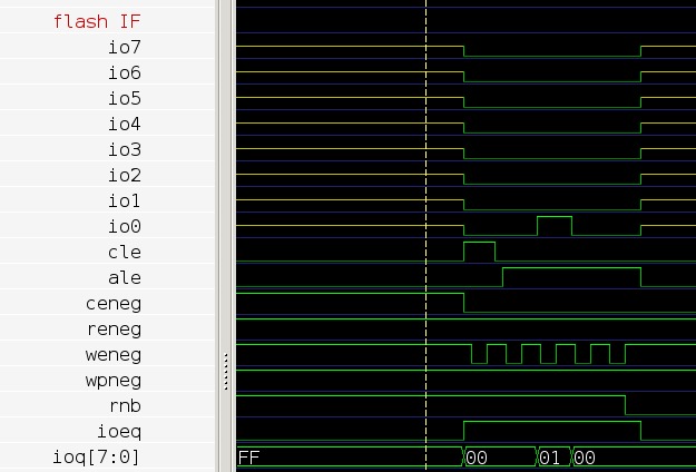
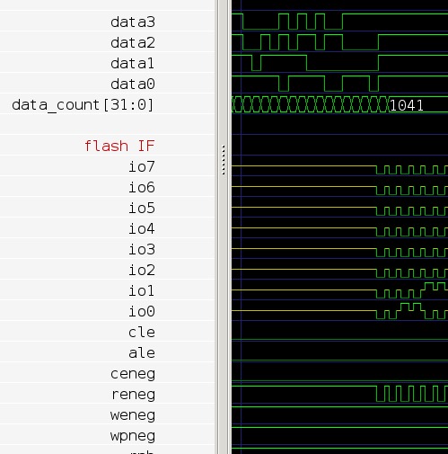
The next wave describes the command latch (cle='1') and
address latch (ale='1') phases on the flash:
-
This wave shows, that right after the SD data
ends, another read from flash starts. This is not
the fastest way to do it, as the flash read
can start earlier. I preferred to wait till SD
transfer completes, to simplify the
design.
-
For more details, please e mail me to
bknpk@hotmail.com .
Put SD flash in the e mail subject.
|