ASIC/FPGA Design and Verification Out Source Services
SD slave with Samsung flash.
-
The existing SD slave
project
was extended recently to support a Samsung flash instead of the
XILINX
ROM components, which are used in the free version of the code.
-
The new design uses a FIFO, build up of XILINX dual port RAM components, in both the direction of SD read from flash and SD write to flash.
It was written in VHDL both design and test-bench.
BASH scripts are used to compile, run, regression and post run checks as well as coverage collection.
The design was mainly simulated and tested using the free VHDL simulator: GHDL. Also simili simulator
was partially used and compilation and simulation (but not regression) scripts are available as well.
simili on this web site
-
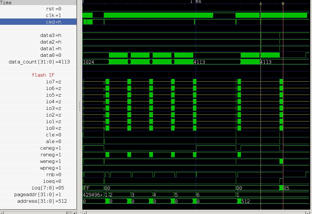
The following wave describes a typical test. First there are simple reads. It is followed by a SD read block.
The two markers are pointing to SD to flash write.
-
For more details, please e mail me to
bknpk@hotmail.com .
Put SD flash in the e mail subject.
-
Related pages to the SD to flash VHDL project:
-
perl SD to flash write check
-
VHDL SD a word about timing
-
perl SD script bit manipulation
-
VHDL function, which generates random numbers
-
checking the IO for legal values while ALE is asserted
-
generating clock for the flash
-
VHDL SD CRC16 function
-
VHDL SD CRC16 RTL
-
SD slave to flash timeout
-
SD slave to flash read burst
-
C++ Reference model for ECC.
|