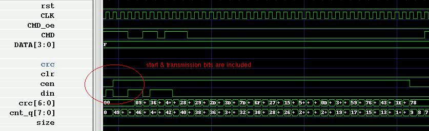
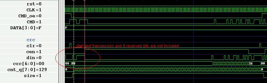
For case 1 and 2 the CRC7 is calculated on 40 bits starting from the very first bit - the start bit. For case 3 the first two bits (start and transmission bits) and the six reserved ones, which follow, are skipped. Than 120 bits are fed to the CRC7 module. In the following waveform a command with 48 bits is the input to the CRC7. The slave module needs to calculate the CRC7 and compare it to what is received from the line. Note the command starts with bits 2'b01.
The case of response with 48 bits is similar. The slave needs to calculate the CRC7 and add it to its response. Note the response starts with bits 2'b00.
Last the case of a response of 136 bits is shown. The slave needs to calculate the CRC7 and add it to its response. Note the response starts with bits 2'b00.
The entire simulation with the above signals as well as others, in VCD format, can be download from the download area at (LAST_REL.vcd.gz)